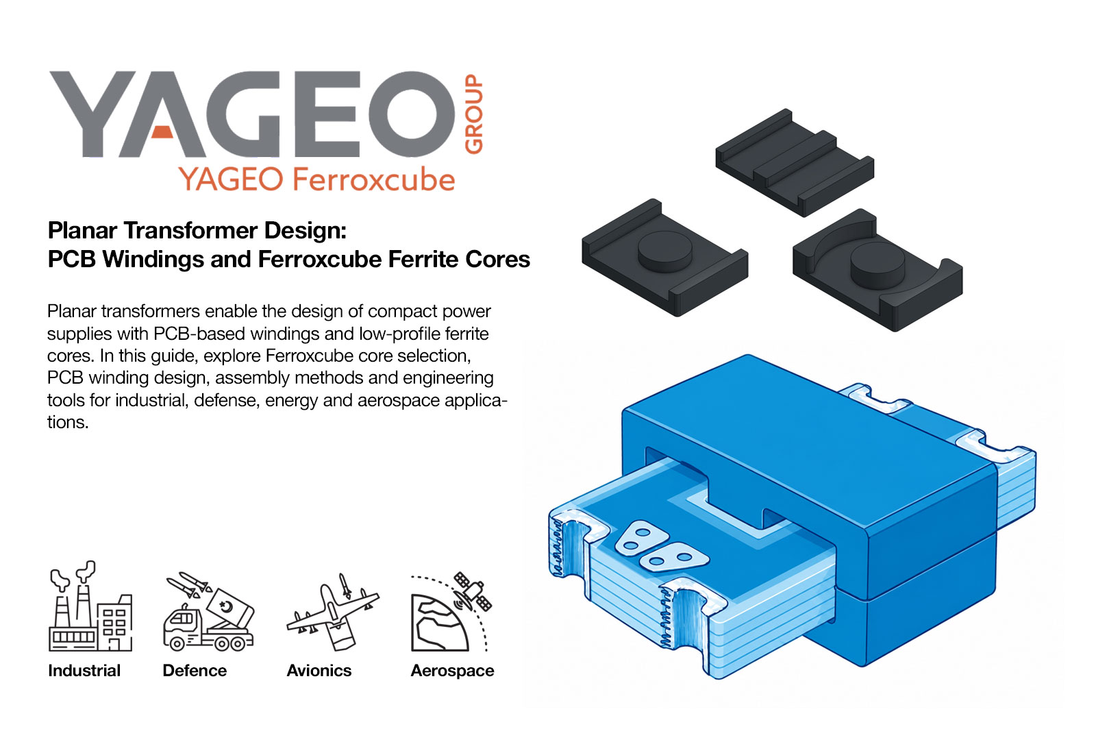
What Is a Planar Transformer?
A planar transformer is a low-profile, high-frequency transformer in which the primary and secondary windings are formed with flat copper layers. In most designs, the windings are implemented as copper traces on a multilayer printed circuit board (PCB). Depending on the application, flat copper plates, copper foil windings, or hybrid winding structures can also be used.
In recent years, the demand for more compact, lower-profile and highly repeatable power electronics has brought planar transformer design into stronger focus. Especially in high-frequency AC-DC and DC-DC power supplies, PCB-wound planar solutions are increasingly evaluated as an alternative to conventional wire-wound transformers. GaN and SiC switching devices, higher power-density targets and production flows that favor automation have made planar transformers a highly relevant option in modern power supply design.
Copper traces on the PCB loop around the center leg of the ferrite core and form the winding turns. The ferrite core parts close around the winding structure from the top and bottom, completing the magnetic path. The high-frequency voltage applied to the primary winding creates a changing magnetic flux in the core; this flux induces voltage in the secondary winding. With the correct topology, turns ratio and insulation structure, the transformer provides both voltage conversion and galvanic isolation.
The PCB-wound transformer approach makes the winding geometry part of the electronic design process. The windings can be placed directly on the main power PCB or built on small additional winding PCBs. This allows the designer to define the number of turns, trace width and layer arrangement in the PCB design environment, reducing the dependency on manual wire-winding work.
Planar transformers are used in isolated DC-DC converters and switched-mode AC-DC power supplies where low height, repeatable winding geometry and high power density are important. Ferroxcube Planar E, Planar ER and EQ ferrite core families provide several geometry options for designers working in industrial, defense, energy, avionics and aerospace applications.
PCB Winding
Primary, secondary and auxiliary windings are created with controlled geometry on PCB layers.
Ferroxcube Core
Planar E, ER and EQ ferrite cores are considered for low-profile power conversion designs.
KiCad Flow
Winding traces, vias, cutouts and manufacturing files can be prepared in the same PCB environment.
Validation
Inductance, temperature, insulation and EMI measurements determine the final design quality.
What Is the Difference Between a Planar Transformer and a Conventional Transformer?
The main difference is the winding geometry and the production method. In a conventional high-frequency transformer, insulated copper wire is wound around a bobbin. In a PCB-based planar transformer, the conductors are formed as copper layers on the printed circuit board. Both structures operate on the principle of electromagnetic induction, but the winding layout affects size, losses, thermal behavior and manufacturing repeatability.
The comparison below refers to high-frequency wire-wound transformers used in switched-mode power supplies. A planar transformer is not a direct drop-in replacement for a 50/60 Hz mains transformer.
| Feature | Conventional Wire-Wound Transformer | PCB-Wound Planar Transformer |
|---|---|---|
| Winding structure | Enamelled wire, litz wire or similar conductors are wound on a bobbin. | Windings are formed as PCB copper traces; layers are connected by vias or terminals. |
| Size and profile | Height depends on the bobbin and winding build-up. | Provides a low profile, but may require a larger horizontal PCB area. |
| Design and production | Requires winding, lead preparation and termination processes. | Winding geometry is part of PCB design; manual winding work can be reduced. |
| Repeatability | Depends on wire placement, winding tension and production method. | Copper trace position and layer stack-up are controlled by PCB manufacturing tolerances. |
| Leakage inductance | Depends on the physical placement and proximity of windings. | Can be reduced by a suitable primary/secondary layer arrangement. |
| Parasitic capacitance | Depends on winding arrangement and insulation structure. | Large overlapping copper areas may increase capacitance; layer order is important. |
| Thermal behavior | Heat transfer from inner windings requires careful design. | Wide copper surfaces can help heat spreading; internal layers and connection losses must be checked. |
| Cost | Depends on winding method, labor, material and production volume. | Winding labor may decrease; multilayer or heavy-copper PCB cost must be considered. |
For design teams, the key benefit is that the winding design can be integrated into the PCB development process. Different winding options can be tested through PCB revisions, while ferrite core assembly, electrical testing and production validation remain part of the overall process.
A planar structure does not automatically mean higher efficiency. The advantages appear when the correct Ferroxcube ferrite material, copper thickness, layer arrangement and mechanical assembly are selected together.
How Does a Planar Transformer Work?
A planar transformer works with primary and secondary windings magnetically coupled through a ferrite core. A high-frequency switching voltage applied to the primary winding creates a changing magnetic flux in the core. This flux induces voltage in the secondary winding and enables power transfer. Unlike a conventional transformer, the windings are implemented with PCB copper traces or flat copper conductors.
Switching the Input Voltage
In DC-DC converters, the input DC voltage is switched at high frequency by power transistors driven by the control circuit. In AC-DC supplies, the mains voltage is first rectified and then delivered to the switching stage. The primary winding receives voltage pulses according to the selected topology. A planar transformer must not be connected directly to a steady DC voltage.
Role of the Ferrite Core and PCB Windings
The copper traces loop around the center leg of the ferrite core and form the turns. Windings on different PCB layers can be connected in series or in parallel. The ferrite core provides the magnetic path that couples the primary and secondary windings. The number of turns, the core cross-section and the applied volt-second determine the flux density in the core.
How Does Turns Ratio Affect Voltage?
In the ideal transformer model, the induced voltage ratio follows the turns ratio: Vs / Vp = Ns / Np. Increasing the secondary turns increases the induced secondary voltage for the same primary voltage. However, the final regulated DC output voltage also depends on topology, duty cycle, control method and losses.
Energy Transfer to the Output
Energy transfer timing depends on the converter topology. In forward and bridge converters, energy is transferred while the primary is driven. In a flyback converter, energy is stored in the magnetic structure while the switch is on and transferred to the output when the switch turns off. This is why the air gap and winding arrangement must be designed for the selected topology.
On the secondary side, diodes or synchronous rectifier MOSFETs rectify the voltage and the output filter reduces ripple. When the insulation structure is designed correctly, the planar transformer provides galvanic isolation between input and output.
What Are the Advantages of Planar Transformers?
Planar transformers are preferred when compact size, repeatability and controlled winding geometry are important. Their main advantage is not a single parameter, but the ability to combine mechanical, electrical and production-related benefits in one structure.
1. Winding Design Can Be Done In-House
The winding becomes part of the PCB design. The designer can define turns, trace widths, layer order and interconnections in KiCad, Altium or another PCB tool. This reduces dependency on external manual winding processes and makes prototypes easier to revise.
2. Manual Winding Labor Can Be Reduced
In conventional transformers, winding, lead preparation and termination introduce labor and variation. In planar structures, a significant part of this work is transferred to PCB manufacturing. This supports more repeatable production, especially in medium and high-volume designs.
3. Low Profile and Compact Power Modules
Planar transformers can achieve very low height compared with many wire-wound alternatives. This is valuable in compact DC-DC modules, distributed power architectures, low-profile industrial supplies and avionics or aerospace electronics where volume and height are tightly constrained.
4. Consistent Winding Geometry in Production
PCB traces are manufactured with controlled dimensions and positions. This makes the winding geometry more repeatable than manual winding, improving consistency from prototype to series production.
5. Leakage Inductance and Coupling Can Be Controlled
The layer order of primary and secondary windings directly affects leakage inductance and coupling. Proper interleaving can reduce leakage inductance, while spacing and shielding choices help manage parasitic capacitance and EMI.
6. Heat Spreading and High-Current Design Are Supported
Wide copper areas, heavy copper layers and parallel layer connections can support high-current secondary windings. PCB copper also provides a useful path for heat spreading when the layout is designed carefully.
7. Prototyping and Product Variants Become Easier
Different turns ratios, layer orders and current ratings can be tested by changing the winding PCB or the winding area in the main PCB. This makes planar transformers attractive for design teams that develop several power supply variants from one platform.
In summary, planar transformers can reduce manual winding effort, provide low profile, improve repeatability and give the designer direct control over the winding geometry. The final benefit depends on the ferrite core, material, PCB stack-up and validation process.
What Are the Disadvantages and Design Considerations of Planar Transformers?
Planar transformers offer important advantages, but they are not automatically the best choice for every power supply. PCB layer count, copper thickness, insulation, capacitance and assembly tolerances must be considered from the beginning.
PCB Layer Count and Manufacturing Cost
More turns or higher current often require more layers, wider copper areas or heavier copper. This can increase PCB cost. In some designs, an additional small winding PCB may be more cost-effective than increasing the layer count of the entire main board.
Number of Turns and Available Area
PCB windings require area. Very high turns counts can become difficult in a limited footprint. The ferrite core window, PCB trace spacing and insulation requirements must be checked together.
Interwinding Capacitance and EMI
Wide overlapping primary and secondary copper layers may increase parasitic capacitance. This can affect common-mode noise and EMI behavior, especially in high dv/dt designs using fast switching devices.
High-Frequency Copper Losses
DC resistance is only one part of the loss picture. At high frequency, skin effect and proximity effect influence copper losses. Winding width, layer arrangement and current sharing must be evaluated carefully.
Insulation and Mechanical Fit
Creepage, clearance, dielectric strength, PCB slots, insulation films, adhesive thickness and ferrite window height must all be managed. A small mechanical mismatch can change the magnetic gap and therefore the inductance.
These are design considerations rather than reasons to avoid planar transformers. With the right core, PCB stack-up and validation process, the advantages usually outweigh the challenges in compact high-frequency power designs.
Where Are Planar Transformers Used?
Planar transformers are used in applications that require low profile, high-frequency operation, controlled production and compact isolated power conversion. They are particularly relevant in industrial, defense, energy, avionics and aerospace electronics.
Why Are Planar Transformers Used in Industrial Power Supplies?
Industrial systems often require reliable isolated power in a limited PCB area. Planar transformers can be used in:
- Isolated supplies for PLC I/O modules and industrial control boards.
- Auxiliary supplies for sensor, measurement and data-acquisition circuits.
- Robotics, servo drives and motor-control units.
- Board-level isolated DC-DC converters and compact power modules.
Which Defense Electronics Circuits Can Use Planar Transformers?
Defense electronics may benefit from low height, repeatable assembly and controlled mechanical construction. Typical areas include:
- Power modules for field communication equipment and portable electronic systems.
- Isolated DC-DC supplies for platform electronics.
- Control and auxiliary power boards for radar and electro-optical systems.
- Power supplies for test, measurement and data-processing equipment.
Where Can Planar Transformers Be Used in Energy Systems?
- Solar and energy-storage converters with isolated DC-DC stages.
- Battery chargers and bidirectional power conversion modules.
- Auxiliary supplies for inverter and UPS control circuits.
- Isolated gate-driver supplies for IGBT, SiC and MOSFET power stages.
What Is the Advantage in Avionics?
Avionics systems value low weight, low profile and repeatable construction. Planar transformers can support compact isolated power modules, but final suitability must be confirmed through the project-specific environmental, EMI and safety requirements.
Can Planar Transformers Be Used in Space and Satellite Electronics?
Planar transformer technology can be considered in space and satellite electronics where low profile and controlled geometry are attractive. However, material selection, outgassing, radiation, mechanical stress and qualification requirements must be handled according to the applicable program rules.
Which Power Converter Topologies Use Planar Transformers?
Planar transformers can be used in flyback, forward, push-pull, half-bridge, full-bridge, phase-shifted full-bridge, LLC and isolated gate-driver supply topologies. The core, turns ratio, air gap and winding stack must be selected according to the topology.
What Is the Mechanical Structure of a Planar Transformer?
A planar transformer is formed by a ferrite core set, one or more flat winding layers, insulation materials and a mechanical fixing method such as clips, adhesive or a housing. The ferrite core surrounds the PCB winding and creates the magnetic path.
Main Parts of a Planar Transformer
| Part | Function |
|---|---|
| Ferrite core | Provides the magnetic path. Ferroxcube Planar E, ER and EQ geometries can be used depending on the design. |
| PCB winding stack | Contains primary, secondary and auxiliary windings as copper traces or copper areas. |
| Optional copper plate or foil | Supports low-resistance high-current windings, typically on low-voltage secondary sides. |
| Insulation layers | Provide electrical separation and help meet creepage, clearance and dielectric strength requirements. |
| Terminals and pads | Connect the windings to the surrounding power circuit. |
| Clip, adhesive or housing | Fixes the ferrite core parts and maintains mechanical alignment. |
How Does the Ferrite Core Fit Around the PCB?
The center leg of the core passes through a cutout or window in the PCB. The outer legs close around the winding area. In some structures the outer legs run outside the board edge; in others, slots or cutouts are used. Mechanical tolerances must leave enough clearance for assembly without stress.
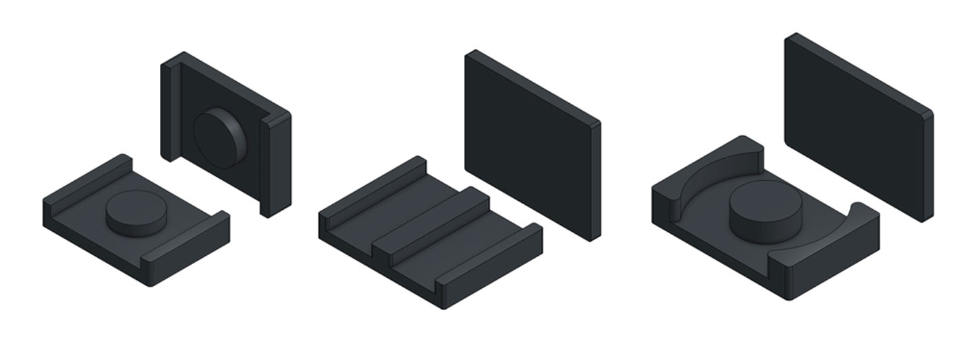
E+E and E+PLT Core Structures
Planar designs may use E+E core sets or E+PLT combinations. E+PLT structures can help reduce height, while E+E structures may provide different window and assembly options depending on the geometry. The actual choice must be based on the selected Ferroxcube core drawing and the winding stack height.
Can the Main PCB and Additional Winding Boards Be Used Together?
Yes. The main PCB can carry part of the winding or only the power circuit, while one or more small winding PCBs are added inside the ferrite window. The total thickness of the main board, winding boards, insulation films, solder and copper layers must fit inside the core window.
The winding stack must not prevent the ferrite core from seating properly. Unintended gaps can change inductance and losses. Any required air gap should be defined by design, not by accidental adhesive or PCB thickness.
What Is the Structure of a PCB Winding in a Planar Transformer?
In a planar transformer, the winding is implemented with copper traces on PCB layers instead of round copper wire. Primary, secondary and auxiliary windings can be placed on different layers with controlled width, spacing and geometry.
Which Layers Form a PCB Winding?
| Layer / Area | Purpose |
|---|---|
| Primary layers | Transfer input energy into the magnetic field. Copper thickness, trace width and parallel layers are selected based on current. |
| Secondary layers | Carry the induced energy to the output. Wide copper areas are common in low-voltage high-current outputs. |
| Auxiliary windings | Supply controllers, feedback circuits, gate drivers or auxiliary outputs. |
| Insulation layers | Provide required separation between primary and secondary circuits. |
| Via connections | Connect turns between layers. Current capacity depends on via count and placement. |
The design is not only about the number of turns. Layer order, winding direction, start/end points, insulation distances, thermal spreading and EMI behavior must be considered together.
What Winding Structures Can Be Used Instead of PCB Windings?
PCB windings are the most common approach, but they are not the only option. Copper foil, copper plates, flexible PCBs and hybrid structures can be selected depending on current level, insulation needs, cost target and mechanical limitations.
| Winding Structure | When to Use | Design Notes |
|---|---|---|
| Standard PCB winding | Repeatable production, compact structure and fast prototyping. | Layer count, copper thickness, insulation and via capacity must be checked. |
| Additional small winding PCBs | When the main PCB does not have enough layers or a modular transformer is preferred. | Total stack height must fit the ferrite core window. |
| Copper foil | High current and low DC resistance requirements. | Insulation film, alignment and terminations must be controlled. |
| Copper plate | Very high current, low-voltage secondary windings. | Cutting tolerances, insulation and thermal expansion must be considered. |
| Flexible PCB | Thin, foldable or mechanically special winding structures. | Cost, assembly sensitivity and bending radius must be evaluated. |
| Hybrid structure | For example, PCB primary with copper-plate secondary. | Electrical insulation and mechanical assembly must be validated as a system. |
How Are Electrical Connections Made in a Planar Transformer?
Electrical connections are made through PCB pads, vias, copper areas and terminals. Instead of bringing wire ends out of a bobbin, the winding terminals are usually connected directly to the surrounding power circuit on the PCB.
How Are Primary and Secondary Terminals Connected?
Primary winding terminals can connect to switches, input capacitors or resonant components. Secondary terminals are routed to rectifier diodes, synchronous MOSFETs, output filters or load terminals. High-current outputs require wide copper areas, multiple vias and parallel layer connections.
| Connection Point | Design Purpose |
|---|---|
| Start/end pads | Connect primary, secondary and auxiliary windings to the circuit. |
| Via groups | Share current between layers; multiple vias are used for high current. |
| Wide copper areas | Reduce resistance, improve heat spreading and lower losses. |
| Insulation gaps | Maintain required primary-secondary creepage and clearance. |
| Test points | Provide access for continuity, inductance and insulation tests. |
In planar transformers, correct schematic connectivity is not enough. Current loop area, via capacity, thermal spreading and safety isolation must also be checked in the PCB layout.
How Is the Ferrite Core Mounted on the PCB?
The ferrite core is placed around the PCB winding from the top and bottom. The center leg passes through the PCB opening and the core parts close the magnetic path. The assembly must align the core, keep it mechanically stable and preserve the designed magnetic gap.
Common Assembly Methods
| Method | Purpose | Design Note |
|---|---|---|
| Clip mounting | Mechanically holds the core halves together. | Clip force must hold the core without cracking ferrite. |
| Adhesive bonding | Fixes the core against vibration, shock or loosening. | Adhesive thickness must not unintentionally change the magnetic gap. |
| Clip and adhesive together | Used where higher mechanical security is needed. | Application area, curing and pressure must be validated together. |
| Mechanical holder or housing | Aligns or protects the transformer as a module. | Thermal expansion and insulation clearances must be considered. |
Mechanical checks should include center-leg clearance, outer-leg seating, stack height, insulation films and possible additional winding PCBs. If the core does not close properly, inductance may change and unintended losses can occur.
Where Should Adhesive Be Applied in a Planar Transformer?
Ferrite core bonding should not be treated as a simple mechanical operation. Adhesive location, thickness and curing method can affect inductance, mechanical strength and long-term reliability. In general, adhesive is applied as a thin controlled layer on the outer-leg contact surfaces of the ferrite core.
Unless specifically intended by design, adhesive should not be used to define the magnetic air gap. If a controlled center-leg gap is required, it must be defined mechanically and not left to random adhesive thickness.
Adhesive Application Checks
| Check Point | Explanation |
|---|---|
| Application area | Usually the outer-leg mating surfaces; the center gap area must be evaluated separately. |
| Bond-line thickness | Excess thickness can create unintended magnetic spacing. |
| Surface cleanliness | Dust, oil and process residues reduce bonding quality. |
| Curing conditions | Temperature, time and pressure must follow the adhesive supplier's recommendations. |
| Electrical impact | Inductance, leakage inductance and insulation should be checked after assembly. |
Can Clips and Adhesive Be Used Together?
Yes. Clips provide mechanical pressure and alignment, while adhesive helps maintain long-term positioning under vibration, shock and thermal cycling. This approach can be considered in industrial, defense, avionics and aerospace-oriented projects, provided that mechanical stress, curing and electrical performance are validated.
What Properties Are Required from a Ferrite Core Adhesive?
| Property | Why It Matters |
|---|---|
| Strong adhesion to ferrite | Prevents separation under vibration and shock. |
| Thin controlled bond line | Reduces unintended magnetic gap variation. |
| Temperature resistance | Power transformers can operate at elevated temperature. |
| Moisture and aging resistance | Supports long-term reliability. |
| Thermal expansion compatibility | Reduces interface stress between ferrite and adhesive. |
| Process repeatability | Important for dosing, curing and series production. |
Which Adhesives Performed Well in Ferroxcube Tests?
Ferroxcube evaluated several adhesive systems under thermal cycling, humidity and pressure-related conditions. Adhesives reported with successful results include:
| Adhesive | Note |
|---|---|
| Eccobond 2332-17 | Epoxy-based system reported with successful test results. |
| Eccobond 50248-F15 | One of the options with positive results in ferrite bonding tests. |
| ThreeBond 2273 | Alternative adhesive with successful thermal and mechanical test behavior. |
| 3M DP490 | High-strength adhesive option evaluated in the study. |
| Hysol RE2039 + HD0243 | Two-component system reported with successful results. |
Practical Assembly Recommendation
First check the dry mechanical fit of the PCB winding stack, insulation layers and ferrite core. The core must close without stress and the center leg must pass through the PCB opening with suitable clearance. Then apply a small controlled amount of adhesive to the outer-leg contact surfaces and cure the assembly under controlled alignment or clip pressure.
Adhesive is a useful mechanical aid, but it is not a substitute for magnetic design. Clean surfaces, thin bond lines and final electrical measurements are essential.
How Is the Winding Formed in a Planar Transformer?
A turn is formed when the copper path surrounds the center leg of the ferrite core. The path can remain on one layer or continue to another layer through vias. Multiple turns, multiple windings and different primary-secondary combinations can be created on the same PCB.
Turn Concept in PCB Windings
| Structure | Explanation |
|---|---|
| Single-layer turn | The copper path loops around the core opening on one layer. |
| Multilayer turn | The winding continues between layers through vias. |
| Parallel copper paths | Several layers or traces share high current to reduce resistance and heating. |
| Primary-secondary stack | Layer order affects leakage inductance and capacitive coupling. |
Can Small Additional Winding PCBs Be Used?
Yes. Additional small winding PCBs can be used when the main board does not provide enough layers, when insulation requirements are easier to manage separately, or when a modular magnetic design is preferred. Instead of increasing the layer count of the whole main board, only the transformer area can be built as a dedicated winding PCB.
Benefits of an Additional Winding PCB
| Benefit | Explanation |
|---|---|
| Layer flexibility | A special transformer stack can be created without increasing the main PCB layer count. |
| Prototype speed | Turns ratios and layer arrangements can be tested by changing only the small PCB. |
| Cost control | Only the winding area may require a special PCB process. |
| Modular design | Different transformer variants can be tested on the same main power board. |
| Insulation optimization | Primary-secondary separation can be managed more flexibly. |
How Is a Separate Winding PCB Added to the Main PCB?
The AC-DC or DC-DC power circuit can remain on the main PCB, while a small winding PCB is mounted in the transformer area. The ferrite core closes around the main PCB and the winding PCB stack. Connection methods include solder pads, castellated edges, pins, terminals or wide copper contact areas.
The main advantage is flexibility: the power circuit can remain unchanged while the transformer winding PCB is revised for different turns ratios, current ratings or layer arrangements.
What Can an Example Planar Transformer Winding Stack Look Like?
The winding stack defines the order of primary and secondary layers inside the PCB or additional winding boards. It affects turns ratio, leakage inductance, parasitic capacitance, insulation strength and thermal behavior.
| Example Stack | Description | Typical Use |
|---|---|---|
| Primary / Insulation / Secondary | Simple and clear separation between primary and secondary. | Basic prototypes and low-to-medium power designs. |
| Primary / Secondary / Primary | Secondary layer is placed between primary layers to reduce leakage inductance. | High-frequency DC-DC converters. |
| Secondary / Primary / Secondary | High-current secondary is divided into two layers for current sharing. | Low-voltage high-current outputs. |
| Main PCB + winding PCB | Transformer winding is built as a replaceable small PCB. | Prototype development and modular variants. |
How Is a PCB Winding Drawn?
Start with ferrite core selection. After the center-leg size, window area and stack height limits are defined, create the PCB opening for the core. Then draw the primary, secondary and auxiliary winding traces around this opening. Each turn should be considered as a current path surrounding the core center leg.
Key Geometrical Parameters
| Parameter | Effect on Design |
|---|---|
| Number of turns | Affects turns ratio, magnetizing inductance and flux density. |
| Trace width | Controls current capacity, DC resistance and temperature rise. |
| Trace spacing | Important for manufacturability, insulation and parasitic capacitance. |
| Copper thickness | Affects resistance and thermal performance. |
| Core cutout | Allows the ferrite center leg to pass through the PCB. |
| Via count and placement | Determines current transfer and heat distribution between layers. |
| Layer order | Controls leakage inductance, capacitive coupling and insulation behavior. |
Do PCB Windings Have to Be Spiral?
No. The copper path does not have to be a classic spiral. What matters is that it surrounds the ferrite center leg and creates the required electrical turns. The geometry can be spiral, rectangular, oval, multilayer, plate-like or a custom wide copper shape.
What Should Be Considered in PCB Winding Design?
Current capacity, insulation, thermal behavior and manufacturability are the main topics. Copper width should be evaluated with AC losses, skin effect and proximity effect in mind. High-frequency layouts also require control of leakage inductance, parasitic capacitance and EMI paths.
Which Software Can Be Used for Planar Transformer Design?
No single tool covers every step of planar transformer design. The process includes power circuit design, PCB winding layout, magnetic calculation, parasitic analysis, thermal behavior and manufacturing documentation. A practical flow combines a PCB CAD tool with magnetic and electromagnetic simulation when needed.
The Most Practical Option: KiCad
KiCad is a practical starting point for drawing planar transformer windings. It supports multilayer PCB design, Gerber outputs, cutouts, custom footprints and Python scripting. The main AC-DC or DC-DC circuit and the transformer winding can be designed in the same environment.
| Tool | Use | Role in Planar Transformer Design |
|---|---|---|
| KiCad | PCB drawing, multilayer windings, Gerber generation. | Practical starting point for main power PCB and winding PCB. |
| Altium Designer | Professional PCB design and advanced stack-up management. | Useful for complex multilayer power boards and team workflows. |
| Ansys Maxwell | Magnetic field, flux density, inductance and saturation analysis. | Validates ferrite geometry, leakage flux and winding placement. |
| Ansys Electronics Desktop | Integrated electromagnetic and system-level workflow. | Combines Maxwell, Q3D and other modules for professional validation. |
| COMSOL Multiphysics | Magnetic, thermal and multiphysics analysis. | Useful when losses, heat and environmental effects are studied together. |
| Altair Flux | Electromagnetic field analysis. | Can analyze magnetic behavior of transformers and inductors. |
| Q3D Extractor | Parasitic resistance, inductance and capacitance extraction. | Evaluates high-frequency parasitics of PCB windings. |
| FastHenry | Resistance and inductance extraction for 3D conductors. | Can support conductor-loss and inductance analysis, but not capacitance extraction. |
In short: KiCad or Altium is used to draw the physical PCB winding; Ansys Maxwell, COMSOL or Altair Flux can validate magnetic and thermal behavior; Q3D or FastHenry can support high-frequency parasitic analysis.
What Is a Practical Workflow for Planar Transformer Design?
A good workflow starts with electrical targets: input/output voltage, power level, isolation requirement, operating frequency and topology. Next, a suitable Ferroxcube core and ferrite material are selected. The first turns calculation is made, the PCB winding is drawn, the mechanical stack is checked and prototypes are measured.
| Application Area | Recommended Starting Setup | Advanced Validation Setup |
|---|---|---|
| Industrial | KiCad or Altium, Ferroxcube catalogs, LCR meter, oscilloscope, thermal camera. | Ansys Maxwell or Q3D for leakage and parasitic checks. |
| Defense | Controlled PCB stack-up, Ferroxcube core and mechanical assembly validation. | Ansys Maxwell, Q3D, EMI measurement, vibration and temperature cycling validation. |
| Avionics | Low-profile core selection and insulation/creepage-clearance review. | Ansys Maxwell, COMSOL, Q3D, thermal analysis and EMI pre-compliance. |
| Aerospace | Controlled material selection, repeatable PCB winding and mechanical fixing. | Magnetic, thermal, mechanical and parasitic analysis as a combined process. |
KiCad Plugins, Guides and Ferroxcube Catalogs for Planar Transformer Design
There is no verified official KiCad plugin dedicated specifically to Ferroxcube planar transformers. However, Ferroxcube core dimensions can be used very effectively in KiCad by creating the correct PCB cutouts, keepouts, footprints and winding geometries.
| Tool / Approach | Use | How It Works with Ferroxcube |
|---|---|---|
| KiCad PCB Editor | Draw winding traces, vias, layers and board cutouts. | Use Ferroxcube catalog dimensions to define the core opening and winding area. |
| KiCad Footprint Editor | Create a custom footprint or mechanical reference for the transformer area. | Define center-leg, outer-leg and keepout areas for the selected core. |
| KiCad Python scripting | Generate repetitive spiral or rectangular winding shapes. | Enter Ferroxcube core dimensions as script parameters. |
| Planar winding generator scripts | Generate planar winding geometries automatically. | Use center-leg size, trace width, spacing and turns as inputs. |
| DXF / mechanical import | Import mechanical references into PCB layout. | Helps align the PCB winding to Ferroxcube mechanical drawings. |
Main Ferroxcube Resources
| Resource | Use |
|---|---|
| Ferroxcube General Catalogue | Main reference for E, ER and EQ core families, dimensions, AL values and accessories. |
| Design of Planar Power Transformers | Technical guide for planar transformer design principles and layer examples. |
| Ferroxcube Material Data | Used to select 3C95, 3C97, 3F36, 3F37, 3F4, 3F46 and other materials. |
| Gluing of Ferrite Cores | Reference for adhesive selection, surface preparation and bonding reliability. |
Which Programs Are Most Suitable for Ferroxcube Planar Transformer Design?
The best program depends on the design stage. Ferroxcube catalogs and material data are the starting point for core and material selection. KiCad is the most practical entry point for PCB windings, while Altium Designer is strong in corporate multilayer PCB workflows. For high-power or critical designs, Ansys Maxwell, Q3D Extractor and COMSOL become important validation tools.
| Design Level | Recommended Toolchain | Purpose |
|---|---|---|
| Fast prototype | Ferroxcube catalog + KiCad + LCR meter + oscilloscope. | First winding geometry, core fit and basic inductance verification. |
| Professional industrial design | Ferroxcube catalog + KiCad/Altium + thermal camera + impedance/LCR measurement. | Production repeatability, temperature rise and efficiency validation. |
| High-power design | KiCad/Altium + Ansys Maxwell + Q3D + thermal camera + EMI measurement. | Leakage inductance, parasitics, high-current paths and EMI behavior. |
| Defense, avionics and aerospace | Ferroxcube documentation + Altium/KiCad + Maxwell + Q3D + COMSOL + environmental and EMI validation. | Magnetic, thermal, mechanical and electrical risks are evaluated together. |
Which Tools Are Needed for Professional and High-Power Planar Transformer Design?
In professional or high-power designs, the goal is not only to make the transformer work. The core must avoid saturation, copper and core losses must remain controlled, temperature rise must stay within safe limits, insulation must be protected and EMI behavior must be manageable.
| Tool / Measurement | What It Checks | Design Impact |
|---|---|---|
| Ansys Maxwell | Magnetic field, flux density, inductance, leakage flux and saturation risk. | Core choice, turns count, air gap and winding placement are validated. |
| Q3D Extractor | Parasitic resistance, inductance and capacitance. | Layer order, overlap area, vias and EMI risk are evaluated. |
| COMSOL Multiphysics | Magnetic, thermal and multiphysics effects. | Hot spots, heat spreading and loss distribution can be studied. |
| Impedance analyzer | Inductance, leakage inductance, resonance and frequency-dependent impedance. | Simulation results are compared with real prototype measurements. |
| Thermal camera | Temperature distribution on PCB winding, ferrite core, vias and nearby components. | Copper area, cooling and current sharing decisions can be improved. |
| EMI measurement | Conducted and radiated emissions, common-mode noise and filter needs. | Winding stack, shielding, snubbers, filters and PCB layout are optimized. |
A recommended sequence is: select the Ferroxcube core and material, design the PCB winding, check magnetic behavior in Maxwell, analyze parasitics with Q3D when necessary, validate thermal behavior with COMSOL or measurements, then test the prototype with impedance, thermal and EMI equipment.
Which Resources Help with Circuit and Magnetic Design?
A successful planar transformer design requires both magnetic design resources and circuit design references. The circuit topology, controller IC, switching frequency, isolation requirement, ferrite material, winding stack, layout and EMI behavior must be evaluated together.
| Resource Type | Use | Contribution to Design |
|---|---|---|
| Ferroxcube General Catalogue | Core dimensions, AL values, materials and accessories. | Core selection and mechanical fit. |
| Ferroxcube Material Data | Loss and frequency behavior of ferrite materials. | Material selection for the operating frequency and temperature range. |
| Controller IC datasheets | PWM operation, duty-cycle limits, protection and recommended topologies. | Determines volt-second limits, switching frequency and transformer operating range. |
| Application notes | Topology design steps, snubber suggestions and feedback loop guidance. | Helps size the transformer for real circuit conditions. |
| Reference designs | Examples with similar power level, input/output voltage or isolation needs. | Useful for comparison of turns ratio, layout, EMI filters and thermal approach. |
| Safety standards | Creepage, clearance and dielectric requirements. | Guides primary-secondary separation and insulation structure. |
| PCB manufacturer rules | Trace width, spacing, copper thickness, via and slot limits. | Ensures the PCB winding is manufacturable. |
Which KiCad Tools Are Used to Create Planar Transformer Windings?
KiCad does not require a special transformer module to create a planar winding. Standard copper traces, zones, vias, layer rules, cutouts, keepouts and scripting tools can be used. Ferroxcube dimensions are taken from the catalog and transferred into the PCB design.
| KiCad Tool | Use | Short Scenario |
|---|---|---|
| PCB Editor | Creates winding traces, vias, layers and board openings. | Define the core cutout and route the windings around it. |
| Route Tracks | Draws spiral, rectangular or custom winding traces. | Manual primary or auxiliary winding creation. |
| Copper Zone | Creates wide copper areas. | High-current secondary winding as a copper plane-like shape. |
| Via and via arrays | Connect layers and share current. | Use multiple vias for high-current layer transitions. |
| Board Setup / Design Rules | Defines trace width, spacing, via size and net classes. | Different rules for primary, secondary and insulation distances. |
| Footprint Editor | Creates a mechanical reference for the core area. | Define center-leg, outer-leg and keepout geometry. |
| Edge.Cuts / Board cutout | Creates the core opening or slots. | Add the cutout for the ferrite center leg. |
| Keepout Area | Protects core, clip or insulation areas from copper or vias. | Prevent unwanted copper under core contact areas. |
| DXF import | Imports mechanical references. | Align the winding to a Ferroxcube drawing. |
| 3D Viewer | Checks mechanical fit visually. | Inspect ferrite, PCB, winding boards and surrounding components. |
| KiCad Python scripting | Automates repetitive winding geometries. | Quickly generate variants with different turns, widths and spacings. |
In short, KiCad can create planar transformer windings using tracks, copper zones, vias, board cutouts, keepouts, footprints and Python scripting. When Ferroxcube catalog dimensions are transferred accurately, KiCad becomes a practical and powerful environment for planar transformer prototypes.
References and Supporting Technical Documents
- Ferroxcube, General Catalogue.
- Ferroxcube, Design of Planar Power Transformers.
- Ferroxcube, Gluing of Ferrite Cores.
- Ferroxcube, Extreme Ferrites for Extreme Conditions: 3C95 / 3C97.
- Ferroxcube, Ferrite Materials for Power Conversion.
- Ferroxcube, Planar E Cores.
- Ferroxcube, Planar ER Cores.
- Ferroxcube, EQ Cores.
- KiCad Planar Winding Generator, GitHub Repository.
- TI, Designing Planar Magnetics.
